Digital-electronics 简明教程
Digital Arithmetic Circuits
本章中,我们将探讨诸如二进制加法器和二进制减法器等基本的算术电路。这些电路可以使用二进制值 0 和 1 进行运算。
In this chapter, let us discuss about the basic arithmetic circuits like Binary adder and Binary subtractor. These circuits can be operated with binary values 0 and 1.
Binary Adder
最基本的算术运算就是加法。执行两个二进制数加法的电路称为 Binary adder 。首先,我们实现一个加法器,执行两个位的加法。
The most basic arithmetic operation is addition. The circuit, which performs the addition of two binary numbers is known as Binary adder. First, let us implement an adder, which performs the addition of two bits.
Half Adder
半加法器是一个组合电路,它执行两个二进制数 A 和 B 的加法,为 single bit 。它产生两个输出和,S 和进位,C。
Half adder is a combinational circuit, which performs the addition of two binary numbers A and B are of single bit. It produces two outputs sum, S & carry, C.
半加法器的 Truth table 如下所示。
The Truth table of Half adder is shown below.
Inputs |
Outputs |
A |
B |
C |
S |
0 |
0 |
0 |
0 |
0 |
1 |
0 |
1 |
1 |
0 |
0 |
1 |
1 |
1 |
1 |
0 |
当我们对两个位进行加法时,最终和的取值范围可以是从 0 到 2(十进制)。我们可以用二进制中的一个位来表示十进制数字 0 和 1。但是,我们无法用二进制中的一个位来表示十进制数字 2。所以,我们需要两个位来用二进制表示它。
When we do the addition of two bits, the resultant sum can have the values ranging from 0 to 2 in decimal. We can represent the decimal digits 0 and 1 with single bit in binary. But, we can’t represent decimal digit 2 with single bit in binary. So, we require two bits for representing it in binary.
令和,S 为最低有效位,进位,C 为最终和的最高有效位。对于前三个输入组合,进位,C 为零,并且 S 的值将基于输入处出现的 number of ones 而为零或一。但是,对于输入的最后一个组合,进位,C 为一,和,S 为零,因为最终和为二。
Let, sum, S is the Least significant bit and carry, C is the Most significant bit of the resultant sum. For first three combinations of inputs, carry, C is zero and the value of S will be either zero or one based on the number of ones present at the inputs. But, for last combination of inputs, carry, C is one and sum, S is zero, since the resultant sum is two.
从真值表中,我们可以直接写出每个输出的 Boolean functions ,如下所示:
From Truth table, we can directly write the Boolean functions for each output as
\mathrm{S \: = \: A \: \oplus \: B}
\mathrm{C \: = \: AB}
我们可以用 2 输入异或门和 2 输入与门来实现以上功能。半加法器的 circuit diagram 如下图所示。
We can implement the above functions with 2-input Ex-OR gate & 2-input AND gate. The circuit diagram of Half adder is shown in the following figure.
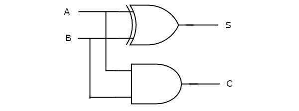
在上述电路中,一个 2 输入异或门和一个 2 输入与门分别产生和,S 和进位,C。因此,半加法器对两个位执行加法操作。
In the above circuit, a two input Ex-OR gate & two input AND gate produces sum, S & carry, C respectively. Therefore, Half-adder performs the addition of two bits.
Full Adder
全加法器是一个组合电路,它执行 addition of three bits A,B 和 Cin。其中,A 和 B 是两个并行有效位,而 Cin 是从前一阶段生成的进位位。此全加法器也产生两个输出和,S 和进位,Cout,它们与半加法器类似。
Full adder is a combinational circuit, which performs the addition of three bits A, B and Cin. Where, A & B are the two parallel significant bits and Cin is the carry bit, which is generated from previous stage. This Full adder also produces two outputs sum, S & carry, Cout, which are similar to Half adder.
全加法器的 Truth table 如下所示。
The Truth table of Full adder is shown below.
Inputs |
Outputs |
A |
B |
Cin |
Cout |
S |
0 |
0 |
0 |
0 |
0 |
0 |
0 |
1 |
0 |
1 |
0 |
1 |
0 |
0 |
1 |
0 |
1 |
1 |
1 |
0 |
1 |
0 |
0 |
0 |
1 |
1 |
0 |
1 |
1 |
0 |
1 |
1 |
0 |
1 |
0 |
1 |
1 |
1 |
1 |
当我们对三个位进行加法时,最终和的取值范围可以是从 0 到 3(十进制)。我们可以用二进制中的一个位来表示十进制数字 0 和 1。但是,我们无法用二进制中的一个位来表示十进制数字 2 和 3。所以,我们需要两个位来用二进制表示这两个十进制数字。
When we do the addition of three bits, the resultant sum can have the values ranging from 0 to 3 in decimal. We can represent the decimal digits 0 and 1 with single bit in binary. But, we can’t represent the decimal digits 2 and 3 with single bit in binary. So, we require two bits for representing those two decimal digits in binary.
令和,S 为最低有效位,进位,Cout 为最终和的最高有效位。在真值表中填写所有输入组合的输出值非常轻松。只需计算输入中出现的 number of ones 并用输出处的等效二进制数表示即可。如果 Cin 等于零,则全加法器真值表与半加法器真值表相同。
Let, sum, S is the Least significant bit and carry, Cout is the Most significant bit of resultant sum. It is easy to fill the values of outputs for all combinations of inputs in the truth table. Just count the number of ones present at the inputs and write the equivalent binary number at outputs. If Cin is equal to zero, then Full adder truth table is same as that of Half adder truth table.
简化后,我们将得到每个输出的以下 Boolean functions :
We will get the following Boolean functions for each output after simplification.
\mathrm{S \: = \: A \: \oplus \: B \: \oplus \: C_{in}}
\mathrm{c_{out} \: = \: AB \: + \: \left ( A \: \oplus \: B \right ) \: c_{in}}
当输入中出现奇数个 1 时,和,S 等于一。我们知道异或门产生的输出是一个奇函数。因此,我们可以使用两个 2 输入异或门或一个 3 输入异或门来产生和,S。我们可以使用两个 2 输入与门和一个或门来实现进位,Cout。全加法器的 circuit diagram 如下图所示。
The sum, S is equal to one, when odd number of ones present at the inputs. We know that Ex-OR gate produces an output, which is an odd function. So, we can use either two 2input Ex-OR gates or one 3-input Ex-OR gate in order to produce sum, S. We can implement carry, Cout using two 2-input AND gates & one OR gate. The circuit diagram of Full adder is shown in the following figure.
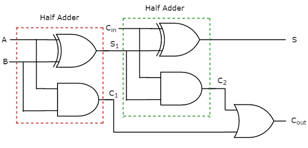
这种加法器称为 Full adder ,因为我们需要两个半加法器和一个或门来实现一个全加法器。如果 Cin 为零,则全加法器变为半加法器。我们可以通过上述电路图或全加法器的输出布尔函数轻松验证这一点。
This adder is called as Full adder because for implementing one Full adder, we require two Half adders and one OR gate. If Cin is zero, then Full adder becomes Half adder. We can verify it easily from the above circuit diagram or from the Boolean functions of outputs of Full adder.
4-bit Binary Adder
4 位二进制加法器执行 addition of two 4-bit numbers 。设 4 位二进制数为$\mathrm{A \: = \: A_{3}A_{2}A_{1}A_{0}}$ 和 $\mathrm{B \: = \: B_{3}B_{2}B_{1}B_{0}}$。我们可以通过以下两种方法之一实现 4 位二进制加法器。
The 4-bit binary adder performs the addition of two 4-bit numbers. Let the 4-bit binary numbers, $\mathrm{A \: = \: A_{3}A_{2}A_{1}A_{0}}$ and $\mathrm{B \: = \: B_{3}B_{2}B_{1}B_{0}}$. We can implement 4-bit binary adder in one of the two following ways.
-
Use one Half adder for doing the addition of two Least significant bits and three Full adders for doing the addition of three higher significant bits.
-
Use four Full adders for uniformity. Since, initial carry Cin is zero, the Full adder which is used for adding the least significant bits becomes Half adder.
目前,我们考虑第二种方法。4 位二进制加法器的 block diagram 如以下数字所示。
For the time being, we considered second approach. The block diagram of 4-bit binary adder is shown in the following figure.
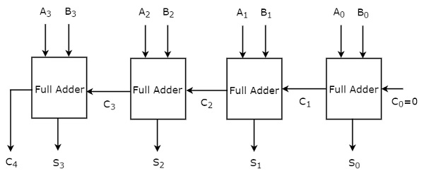
在此,级联了 4 个全加法器。每个全加法器获取两个并行输入 A 和 B 的各个位。一个全加法器的进位输出将成为后续高阶全加法器的进位输入。此 4 位二进制加法器产生的结果和最多有 5 位。因此,最后阶段全加法器的进位输出将是最高有效位。
Here, the 4 Full adders are cascaded. Each Full adder is getting the respective bits of two parallel inputs A & B. The carry output of one Full adder will be the carry input of subsequent higher order Full adder. This 4-bit binary adder produces the resultant sum having at most 5 bits. So, carry out of last stage Full adder will be the MSB.
通过级联所需数量的全加法器,我们可以由此实现任何较高阶的二进制加法器。这种二进制加法器也称为 ripple carry (binary) adder ,因为进位从一个级向下一级传播(脉冲)。
In this way, we can implement any higher order binary adder just by cascading the required number of Full adders. This binary adder is also called as ripple carry (binary) adder because the carry propagates (ripples) from one stage to the next stage.
Binary Subtractor
执行两个二进制数的减法运算的电路称为 Binary subtractor 。我们可以通过以下两种方法实现二进制减法器。
The circuit, which performs the subtraction of two binary numbers is known as Binary subtractor. We can implement Binary subtractor in following two methods.
-
Cascade Full subtractors
-
2’s complement method
在第一种方法中,我们将级联“n”个全减法器来获得一个 n 位二进制减法器。因此,您首先可以实现半减法器和全减法器,类似于半加法器和全加法器。然后,可以通过级联“n”个全减法器来实现一个 n 位二进制减法器。因此,我们将有用于两个二进制数的二进制加法和减法的两个单独电路。
In first method, we will get an n-bit binary subtractor by cascading 'n' Full subtractors. So, first you can implement Half subtractor and Full subtractor, similar to Half adder & Full adder. Then, you can implement an n-bit binary subtractor, by cascading ‘n’ Full subtractors. So, we will be having two separate circuits for binary addition and subtraction of two binary numbers.
在第二种方法中,我们可以通过对第二个输入进行一些修改来使用相同的二进制加法器来减去两个二进制数。因此,在内部执行二进制加法运算,但输出是结果减法。
In second method, we can use same binary adder for subtracting two binary numbers just by doing some modifications in the second input. So, internally binary addition operation takes place but, the output is resultant subtraction.
我们知道,两个二进制数 A 和 B 的减法可以写为,
We know that the subtraction of two binary numbers A & B can be written as,
\mathrm{A-B \: = \: A \: + \: \left ( {2}'s \: compliment \: of \: B \right )}
\mathrm{\Rightarrow \: A \: - \: B \: = \: A \: + \: \left ( {1}'s \: compliment \: of \: B \right ) \: + \: 1}
4-bit Binary Subtractor
4 位二进制减法器产生 subtraction of two 4-bit numbers 。设 4 位二进制数为 $\mathrm{A \: = \: A_{3}A_{2}A_{1}A_{0}}$ 和 $\mathrm{B \: = \: B_{3}B_{2}B_{1}B_{0}}$。在内部,4 位二进制减法器的操作与 4 位二进制加法器类似。如果将二进制数 A 的正常位、二进制数 B 的补码位和初始进位 (借位) Cin 作为一个应用到 4 位二进制加法器,那么它就变成 4 位二进制减法器。4 位二进制减法器的 block diagram 如以下数字所示。
The 4-bit binary subtractor produces the subtraction of two 4-bit numbers. Let the 4bit binary numbers, $\mathrm{A \: = \: A_{3}A_{2}A_{1}A_{0}}$ and $\mathrm{B \: = \: B_{3}B_{2}B_{1}B_{0}}$. Internally, the operation of 4-bit Binary subtractor is similar to that of 4-bit Binary adder. If the normal bits of binary number A, complemented bits of binary number B and initial carry (borrow), Cin as one are applied to 4-bit Binary adder, then it becomes 4-bit Binary subtractor. The block diagram of 4-bit binary subtractor is shown in the following figure.
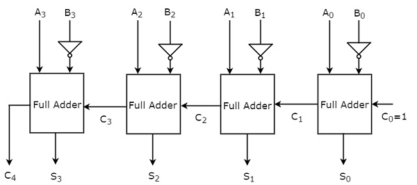
此 4 位二进制减法器产生的输出最多有 5 位。如果二进制数 A 大于二进制数 B,则输出的最高有效位为零,其余位保留 A-B 的大小。如果二进制数 A 小于二进制数 B,则输出的最高有效位为一。因此,对输出取 2 的补码以获得 A-B 的大小。
This 4-bit binary subtractor produces an output, which is having at most 5 bits. If Binary number A is greater than Binary number B, then MSB of the output is zero and the remaining bits hold the magnitude of A-B. If Binary number A is less than Binary number B, then MSB of the output is one. So, take the 2’s complement of output in order to get the magnitude of A-B.
通过级联所需数量的全加法器并进行必要的修改,我们可以由此实现任何较高阶的二进制减法器。
In this way, we can implement any higher order binary subtractor just by cascading the required number of Full adders with necessary modifications.
Binary Adder / Subtractor
可以用来在任何时候对两个二进制数执行加法或减法的电路称为 Binary Adder / subtractor 。二进制加法器和二进制减法器都包含一组级联的全加法器。二进制数 A 的输入位直接应用于二进制加法器和二进制减法器。
The circuit, which can be used to perform either addition or subtraction of two binary numbers at any time is known as Binary Adder / subtractor. Both, Binary adder and Binary subtractor contain a set of Full adders, which are cascaded. The input bits of binary number A are directly applied in both Binary adder and Binary subtractor.
二进制加法器和二进制减法器中全加法器的输入有两个不同。
There are two differences in the inputs of Full adders that are present in Binary adder and Binary subtractor.
-
The input bits of binary number B are directly applied to Full adders in Binary adder, whereas the complemented bits of binary number B are applied to Full adders in Binary subtractor.
-
The initial carry, C0 = 0 is applied in 4-bit Binary adder, whereas the initial carry (borrow), C0 = 1 is applied in 4-bit Binary subtractor.
众所周知,当另一个输入为零时,一个 2-input Ex-OR gate 将生成一个输出,该输出与第一个输入相同。类似地,当另一个输入为一时,它会生成一个输出,该输出是第一个输入的补码。
We know that a 2-input Ex-OR gate produces an output, which is same as that of first input when other input is zero. Similarly, it produces an output, which is complement of first input when other input is one.
因此,我们可以将二进制数 B 的输入位应用于 2 输入异或门。所有这些异或门的另一个输入是 C0。因此,根据 C0 的值,异或门会生成二进制数 B 的法线位或补码位。
Therefore, we can apply the input bits of binary number B, to 2-input Ex-OR gates. The other input to all these Ex-OR gates is C0. So, based on the value of C0, the Ex-OR gates produce either the normal or complemented bits of binary number B.
4-bit Binary Adder / Subtractor
4 位二进制加法器/减法器根据初始进位或借位,即 𝐶0 的值生成两个 4 位数的加法或减法。假设 4 位二进制数为 $\mathrm{A \: = \: A_{3}A_{2}A_{1}A_{0}}$ 且 $\mathrm{B \: = \: B_{3}B_{2}B_{1}B_{0}}$。4 位二进制加法器/减法器的操作类似于 4 位二进制加法器和 4 位二进制减法器。
The 4-bit binary adder / subtractor produces either the addition or the subtraction of two 4-bit numbers based on the value of initial carry or borrow, 𝐶0. Let the 4-bit binary numbers, $\mathrm{A \: = \: A_{3}A_{2}A_{1}A_{0}}$ and $\mathrm{B \: = \: B_{3}B_{2}B_{1}B_{0}}$. The operation of 4-bit Binary adder / subtractor is similar to that of 4-bit Binary adder and 4-bit Binary subtractor.
将外部的二进制数 A 和 B 的法线位以及初始进位或借位 C0 应用于 4 位二进制加法器。4 位二进制加法器/减法器的 block diagram 在下图中显示。
Apply the normal bits of binary numbers A and B & initial carry or borrow, C0 from externally to a 4-bit binary adder. The block diagram of 4-bit binary adder / subtractor is shown in the following figure.
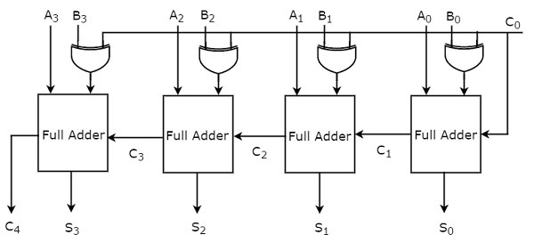
如果初始进位,𝐶0 为零,则每个全加器都会得到二进制数 A 和 B 的法线位。因此,4 位二进制加法器/减法器会生成一个输出,该输出是 A 和 B 的 addition of two binary numbers 。
If initial carry, 𝐶0 is zero, then each full adder gets the normal bits of binary numbers A & B. So, the 4-bit binary adder / subtractor produces an output, which is the addition of two binary numbers A & B.
如果初始借位,𝐶0 为一,则每个全加器都会得到二进制数 A 的法线位和二进制数 B 的补码位。因此,4 位二进制加法器/减法器会生成一个输出,该输出是 A 和 B 的 subtraction of two binary numbers 。
If initial borrow, 𝐶0 is one, then each full adder gets the normal bits of binary number A & complemented bits of binary number B. So, the 4-bit binary adder / subtractor produces an output, which is the subtraction of two binary numbers A & B.
因此,借助额外的异或门,同一个电路可以用于两个二进制数的加法和减法。
Therefore, with the help of additional Ex-OR gates, the same circuit can be used for both addition and subtraction of two binary numbers.