Digital-electronics 简明教程
Digital Electronics - Serial Binary Adder
在数字电子学中, binary adder 是一个组合逻辑电路,它执行两个或多个二进制数字的加法。二进制加法是基于加法的布尔代数定律执行的,即
In digital electronics, the binary adder is a combinational logic circuit which performs the addition of two or more binary digits. The binary addition is performed based on the Boolean algebraic laws of addition, i.e.,
\mathrm{0 \: + \: 0 \: = \: 0}
\mathrm{0 \: + \: 1 \: = \: 1}
\mathrm{1 \: + \: 0 \: = \: 1}
\mathrm{1 \: + \: 1 \: = \: 0}
二进制加法器分为两类,即 serial binary adder 和 parallel binary adder .
Binary adders are classified into two types namely, serial binary adder and parallel binary adder.
在本教程中,我们将讨论串行二进制加法器、其定义、逻辑电路图和操作。因此,让我们从串行二进制加法器的基本介绍开始。
In this tutorial, we will discuss serial binary adder, its definition, logic circuit diagram, and operation. So, let us start with basic introduction of serial binary adder.
What is a Serial Binary Adder?
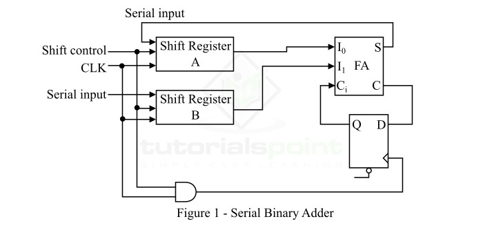
serial binary adder 是一个二进制加法器电路,用于串行形式地添加二进制数字。在串行加法器中,串行相加的两个二进制数字存储在两个移位寄存器中,即移位寄存器 A 和移位寄存器 B。
A serial binary adder is a binary adder circuit which is used to add binary numbers in serial form. In the serial adder, the two binary numbers which are added serially are stored in two shift registers, let shift register A and shift register B.
串行二进制加法器的逻辑电路图如图 1 所示。
The logic circuit diagram of the serial binary adder is shown in Figure 1.

串行加法器电路的各元件功能如下:
The function of different elements of the serial adder circuit is as follows −
Full Adder
全加器是一个数字组合逻辑电路,可以加三个二进制数位并产生两个输出位,即和位和进位位。在串行二进制加法器电路中,全加器一次加一对二进制数位。
Full adder is a digital combinational logic circuit which can add three binary digits and can produce two output bits, i.e. sum bit and carry bit. In the serial binary adder circuit, the full adder adds one pair of bits at a time.
Shift Register
可以存储若干个二进制数位的一组触发器称为移位寄存器。在串行二进制加法器中,使用了两个移位寄存器,一个用于存储被加数的二进制数位,另一个用于存储加数。
A group of flip-flops that can store several bits of data is called a shift register. In serial binary adder, two shift registers are used, where one is for storing augend bit and the other is for storing added of the binary number.
Operation of Series Binary Adder
在串行二进制加法器电路中,使用全加器电路一次加一对二进制数位(比特)。由全加器产生的进位被传送到D触发器。因此,此D触发器的输出随后用作下一对有效数位的进位输入。和位S被传送到第三个移位寄存器。现在,让我们详细了解串行二进制加法器的操作。
In the serial binary adder circuit, the binary digits (bits) are added one pair at a time using a full-adder circuit. The carry generated from the full adder is transferred to a D-flip flop. Thus, the output of this D-flip flop is then used as the carry input for the next pair of significant bits. The sum bit S is transferred to a third shift register. Now, let us understand the operation of the serial binary adder in the detail.
开始时,移位寄存器A存储给定二进制数的被加数数位,移位寄存器B存储加数数位。最初,D触发器被清零,因此不存在进位位。移位寄存器A和B的输出在输入I0和I1处向全加器电路提供一对有效数位。使用移位控制来使移位寄存器A和B以及进位触发器工作。
At beginning, the shift register A stores the augend bit of the given binary number, and the shift register B stores the addend bit. Initially, the D flip flop is cleared to 0, hence no carry bit is present. The outputs of shift registers A and B supply a pair of significant bits to the full adder circuit at inputs I0 and I1. A shift control is used to enable the shift registers A and B and the carry flip-flop.
因此,在每个时钟脉冲时,寄存器A和B向右移位,全加器电路的输出S中的和位进入移位寄存器A的最左端。因此,对于每个后续的时钟脉冲,新的和位被传送到移位寄存器A,并且新的进位位被传送到D触发器的输出Q。此过程将持续到移位控制被禁用为止。
Therefore, at each clock pulse, the registers A and B are shifted to the right, and the sum bit from output S of the full adder circuit enters the left most of the shift register A. Thus, for each succeeding clock pulse a new sum bit is transferred to the shift register A and a new carry bit is transferred to the output Q of the D flip flop. This process continues until the shift control is disabled.
因此,通过向全加器电路提供一对二进制数位和前一个进位,以及一次向移位寄存器A中传输和位,来完成以串行形式对两个二进制数的加法。
Hence, the addition of two binary numbers in serial form is accomplished by supplying a pair of bits together with the previous carry to a full adder circuit, and transferring a sum bit at a time into the shift register A.
现在,我们可以总结串行二进制加法器的操作过程如下:
Now, we can summarize the working process of the serial binary adder as follows −
-
Initially, the shift register A and the carry flip flop are set to 0, and the first number is added from the register B.
-
When the register B is shifting through the full adder, a second number is transferred to it through its serial input.
-
This second number is then added to the number of the register A, while a third number is transferred to into the register B through the serial input.
此过程重复执行,以串行方式对两个或更多个二进制数进行加法,并将和结果累积在移位寄存器A中。
This process is executed repeatedly to perform the addition of two, three, or more binary number in serial form and accumulate the sum result in the shift register A.